
IMARC Group’s latest report, titled “Semiconductor Packaging Market Size, Share, Trends and Forecast by Type, Packaging Material, Technology, End User, and Region, 2025-2033”, offers a comprehensive analysis of the industry, which comprises insights on the semiconductor packaging market. The report also includes competitor and regional analysis, and contemporary advancements in the market. the global semiconductor packaging market size was valued at USD 37.5 Billion in 2024. Looking forward, IMARC Group estimates the market to reach USD 68.2 Billion by 2033, exhibiting a CAGR of 6.81% from 2025-2033. Asia Pacific currently dominates the market, holding a market share of over 54.3% in 2024. Substantial investments in leading-edge packaging technologies, resilient semiconductor manufacturing landscape, and magnifying need for consumer electronics, are contributing to the semiconductor packaging market share expansion.
Request Free Sample Report (Exclusive Offer on this report): https://www.imarcgroup.com/semiconductor-packaging-market/requestsample
Rising Demand for Advanced Packaging Technologies to Support AI and HPC Applications:
One of the most significant trends in the semiconductor packaging industry is the growing adoption of advanced packaging technologies, including fan-out wafer-level packaging (FOWLP), 2.5D and 3D IC integration, and system-in-package (SiP) solutions. With artificial intelligence (AI), high-performance computing (HPC), and 5G networks driving the next wave of technological evolution, semiconductor manufacturers are focusing on enhanced performance, power efficiency, and density optimization through innovative packaging approaches. Traditional wire bonding and flip-chip packaging methods are gradually being replaced by heterogeneous integration techniques, which allow multiple chiplets, memory modules, and logic components to be integrated into a single package. This shift is particularly evident in AI accelerators, GPUs, and advanced processors, where high-speed interconnects and compact designs are critical for maximizing computational efficiency.
Moreover, chiplet-based architectures are gaining traction as an alternative to traditional monolithic chip designs. Leading semiconductor companies, including AMD, Intel, and NVIDIA, are actively developing chiplet-based processors to improve modularity, scalability, and cost efficiency. This approach not only enhances yield rates and performance but also enables the customization of semiconductor solutions for applications ranging from data centers to edge computing devices. As AI-powered applications continue to expand, advanced packaging solutions are expected to play a crucial role in enhancing semiconductor performance, reducing latency, and optimizing power consumption. The increasing collaboration between foundries, packaging houses, and design firms will further accelerate the adoption of cutting-edge packaging innovations, positioning semiconductor packaging as a key enabler of next-generation computing technologies.
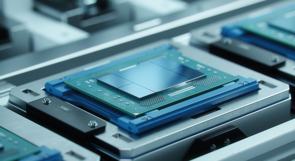
Expanding Role of Heterogeneous Integration and 3D Packaging:
The semiconductor packaging industry is witnessing a paradigm shift toward heterogeneous integration and 3D packaging, allowing multiple semiconductor components to be stacked or integrated into a unified package. Unlike conventional 2D packaging, which relies on side-by-side chip placement, 3D packaging enables vertical stacking, significantly improving performance density, interconnect speeds, and thermal management. This trend is particularly evident in applications such as mobile processors, high-bandwidth memory (HBM) modules, and automotive AI chips, where compact form factors and high-speed processing are essential. Technologies such as through-silicon vias (TSVs) and wafer-level fan-out packaging (WLFO) are enabling the seamless integration of logic, memory, and power management ICs, reducing latency and power consumption while enhancing processing efficiency.
Heterogeneous integration is also gaining traction in 5G, edge AI, and automotive applications, where the demand for multi-functional semiconductor solutions is growing. Companies are increasingly investing in multi-chiplet packaging, hybrid bonding techniques, and embedded passive components, enabling the development of more efficient, high-performance semiconductor solutions. Furthermore, the growing importance of automotive semiconductor packaging is accelerating the adoption of ruggedized, thermally efficient, and high-reliability packaging solutions. With electric vehicles (EVs) and autonomous driving systems requiring advanced semiconductor technologies, manufacturers are focusing on automotive-grade packaging solutions that enhance longevity, reliability, and power efficiency. As the demand for faster, more efficient, and compact semiconductor solutions increases, heterogeneous integration and 3D packaging will continue to redefine the semiconductor packaging landscape, driving innovation and performance optimization across multiple industry verticals.
Increasing Adoption of Sustainable and Cost-Effective Packaging Materials:
With the global semiconductor industry moving toward sustainability, there is a growing emphasis on eco-friendly, cost-efficient, and high-performance packaging materials. Traditional silicon-based packaging substrates are increasingly being supplemented with organic, composite, and advanced polymer materials, enhancing thermal conductivity, electrical performance, and environmental sustainability. One of the most promising developments in this space is the shift toward bio-based and recyclable packaging solutions, aimed at reducing electronic waste (e-waste) and minimizing the carbon footprint of semiconductor production. Leading semiconductor companies are adopting halogen-free, lead-free, and low-power packaging materials, aligning with global sustainability initiatives and regulatory standards.
Additionally, cost efficiency remains a critical factor in the semiconductor packaging market, as manufacturers seek to optimize packaging yields, reduce material costs, and enhance production efficiency. Innovations in wafer-level packaging (WLP), panel-level packaging (PLP), and embedded substrate technologies are helping companies achieve higher throughput rates, lower defect densities, and improved thermal performance. Another significant trend is the integration of advanced cooling solutions, such as liquid-cooled packaging, phase-change materials (PCMs), and advanced thermal interface materials (TIMs). These innovations are essential for high-power AI processors, automotive semiconductor modules, and next-generation HPC applications, where heat dissipation and power efficiency are critical to performance and longevity. As the semiconductor packaging industry continues to evolve, the focus on sustainable, cost-effective, and high-performance packaging solutions will play a crucial role in shaping the future of semiconductor innovation.
Leading Key Players Operating in the Semiconductor Packaging Industry:
- Amkor Technology Inc.
- ASE Group
- ChipMOS Technologies Inc.
- Fujitsu Limited
- Intel Corporation
- International Business Machines Corporation
- Jiangsu Changjiang Electronics Technology Co., Ltd.
- Powertech Technology Inc.
- Qualcomm Incorporated
- Samsung Electronics Co. Ltd.
- STMicroelectronics International N.V.
- Taiwan Semiconductor Manufacturing Company Limited
- Texas Instruments Incorporated
Semiconductor Packaging Market Trends:
The semiconductor packaging market is undergoing a technological transformation, driven by the adoption of advanced packaging architectures, high-speed interconnect solutions, and material innovations. One of the most notable trends is the rise of chiplet-based designs and 3D stacked packaging, enabling higher performance, lower power consumption, and improved space efficiency for semiconductor devices. Companies are moving beyond traditional monolithic chips, leveraging heterogeneous integration and multi-chip solutions to enhance processing power and modularity. Additionally, fan-out and wafer-level packaging (WLP) solutions are gaining popularity, particularly in AI, 5G, and high-performance computing (HPC) applications. These technologies enable higher density interconnects, lower resistance pathways, and enhanced signal integrity, making them ideal for power-intensive semiconductor applications.
Another major trend is the shift toward sustainable semiconductor packaging, with manufacturers exploring recyclable materials, low-energy production methods, and eco-friendly substrate solutions. As regulatory frameworks tighten and environmental concerns rise, semiconductor companies are adopting halogen-free, lead-free, and energy-efficient packaging techniques to minimize waste and environmental impact. The automotive sector is also driving innovation in semiconductor packaging, with the increasing demand for ruggedized, thermally optimized, and high-reliability semiconductor solutions. The rise of electric vehicles (EVs), autonomous driving, and AI-driven automotive systems is accelerating the adoption of specialized automotive semiconductor packaging, ensuring longevity, efficiency, and performance under extreme conditions. With the increasing complexity of semiconductor devices and the growing demand for high-performance computing solutions, the semiconductor packaging market is poised for significant advancements in miniaturization, power efficiency, and cost optimization, positioning it as a crucial component of the future semiconductor ecosystem.
Ask Analyst for Instant Discount and Download Full Report with TOC & List of Figure: https://www.imarcgroup.com/semiconductor-packaging-market
Key Market Segmentation:
Analysis by Type:
- Flip Chip
- Embedded DIE
- Fan-in WLP
- Fan-out WLP
Analysis by Packaging Material:
- Organic Substrate
- Bonding Wire
- Leadframe
- Ceramic Package
- Die Attach Material
- Others
Analysis by Technology:
- Grid Array
- Small Outline Package
- Flat no-leads Package
- Dual In-Line Package
- Others
Analysis by End User:
- Consumer Electronics
- Automotive
- Healthcare
- IT and Telecommunication
- Aerospace and Defense
- Others
Breakup by Region:
- North America (United States, Canada)
- Asia Pacific (China, Japan, India, Australia, Indonesia, Korea, Others)
- Europe (Germany, France, United Kingdom, Italy, Spain, Others)
- Latin America (Brazil, Mexico, Others)
- Middle East and Africa (United Arab Emirates, Saudi Arabia, Qatar, Iraq, Other)
Key Highlights of the Report:
- Market Performance (2019-2024)
- Market Outlook (2025-2033)
- Porter’s Five Forces Analysis
- Market Drivers and Success Factors
- SWOT Analysis
- Value Chain
- Comprehensive Mapping of the Competitive Landscape
About Us:
IMARC Group is a global management consulting firm that helps the world’s most ambitious changemakers to create a lasting impact. The company provide a comprehensive suite of market entry and expansion services.
IMARC offerings include thorough market assessment, feasibility studies, company incorporation assistance, factory setup support, regulatory approvals and licensing navigation, branding, marketing and sales strategies, competitive landscape and benchmarking analyses, pricing and cost research, and procurement research.
Contact Us:
IMARC Group
134 N 4th St. Brooklyn, NY 11249, USA
Email: sales@imarcgroup.com
Tel No:(D) +91 120 433 0800
Americas:- +1 631 791 1145
Also Read – https://fastpanda.in/